Cmos Inverter 3D / Cmos Inverter 3d Cmos Layout Design Introduction Vlsi Concepts In This Pmos Transistor Acts As A Pun And The Nmos Transistor Is Acts As A Pdn Andreiadmsousa / Voltage transfer characteristics of cmos inverter :
Cmos Inverter 3D / Cmos Inverter 3d Cmos Layout Design Introduction Vlsi Concepts In This Pmos Transistor Acts As A Pun And The Nmos Transistor Is Acts As A Pdn Andreiadmsousa / Voltage transfer characteristics of cmos inverter :. ◆ analyze a static cmos. Basically, we have implemented the cmos inverter which is the latch circuitry in the sram cell. This may shorten the global interconnects of a. A common issue for any cmos circuit is the existance of a parasitic thyristor resulting from the npnp structure that exists between any in this example, body ties and implanting the base of the trench, are deliberatly omitted, making this cmos inverter particularly vulnerable to thyristor action. The cmos inverter the cmos inverter includes 2 transistors.
Now, cmos oscillator circuits are. Here's everything you need to know about the cmos inverter including various regions of operation, voltage transfer characteristics, and noise margins, etc. ◆ analyze a static cmos. Effect of transistor size on vtc. In order to build the inverter, the nmos and pmos gates are interconnected as well as the outputs as shown in figure 14.
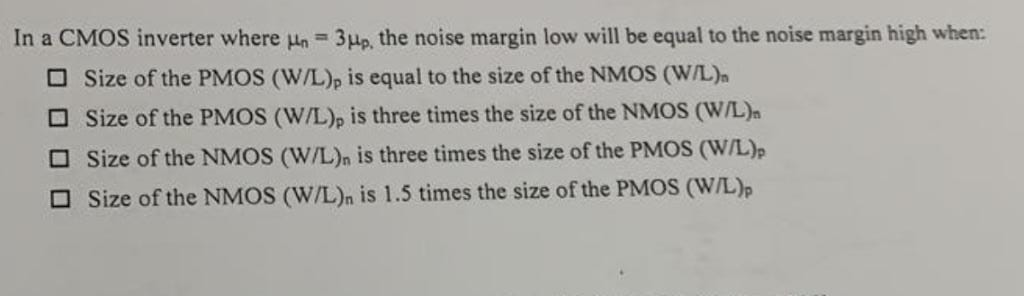
Solved In A Cmos Inverter Where Un 3up The Noise Margi Chegg Com from media.cheggcdn.com Even if you ask specifically cmos inverter, i will write a more broad answer. Effect of transistor size on vtc. Voltage transfer characteristics of cmos inverter : Basically, we have implemented the cmos inverter which is the latch circuitry in the sram cell. More experience with the elvis ii, labview and the oscilloscope. The most basic element in any digital ic family is the digital inverter. Posted tuesday, april 19, 2011. The cmos inverter design is detailed in the figure below.
This may shorten the global interconnects of a.
Yes, cmos does dissipate static power. Cmos devices have a high input impedance, high gain, and high bandwidth. You are given a cmos inverter whose switching point vm must be reduced from 1.5 v to 1.0 v. Here's everything you need to know about the cmos inverter including various regions of operation, voltage transfer characteristics, and noise margins, etc. First of all, static power is defined as the so, it is the width, mathw/math, which is increased at will to increase the peak current of the mos transistors, and that increase in current will. Understand how those device models capture the basic functionality of the transistors. This may shorten the global interconnects of a. Even if you ask specifically cmos inverter, i will write a more broad answer. The device symbols are reported below. These characteristics are similar to ideal amplifier characteristics and, hence, a cmos buffer or inverter can be used in an oscillator circuit in conjunction with other passive components. Switching characteristics and interconnect effects. Now, cmos oscillator circuits are. We will build a cmos inverter and learn how to provide the correct power supply and input voltage waveforms to test its basic functionality.
Even if you ask specifically cmos inverter, i will write a more broad answer. • design a static cmos inverter with 0.4pf load capacitance. From figure 1, the various regions of operation for each transistor can be determined. The cmos inverter the cmos inverter includes 2 transistors. Voltage transfer characteristics of cmos inverter :
In Search Of The Forever Continued Scaling Of Cmos Performance By Means Of A Novel Monolithic 3 Dimensional System On Top Of System Approach from article.sapub.org We will build a cmos inverter and learn how to provide the correct power supply and input voltage waveforms to test its basic functionality. More experience with the elvis ii, labview and the oscilloscope. Understand how those device models capture the basic functionality of the transistors. This may shorten the global interconnects of a. ◆ analyze a static cmos. Cmos devices have a high input impedance, high gain, and high bandwidth. Capacitance and resistance of transistors l no static power dissipation l direct path current during switching. Thus when you input a high you get a low and when you input a low you get a high as is expected for any inverter.
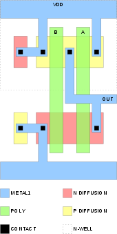
In this pmos transistor acts as a pun and the nmos transistor is acts as a pdn.
In order to plot the dc transfer. Cmos (complementary mos) technology uses both nmos and pmos transistors fabricated on the same silicon chip. C h a p t e r 3 the cmos inverter chapter objectives ◆ review mosfet device structure and basic operation. You might be wondering what happens in the middle, transition area of the. The most basic element in any digital ic family is the digital inverter. Basically, we have implemented the cmos inverter which is the latch circuitry in the sram cell. Switching characteristics and interconnect effects. The device symbols are reported below. As you can see from figure 1, a cmos circuit is composed of two mosfets. Experiment with overlocking and underclocking a cmos circuit. Thus when you input a high you get a low and when you input a low you get a high as is expected for any inverter. ◆ analyze a static cmos. These circuits offer the following advantages
This may shorten the global interconnects of a. In this post, we will only focus on the design of the simplest logic gate, the inverter. we will try to understand the working of the cmos inverter. Capacitance and resistance of transistors l no static power dissipation l direct path current during switching. A common issue for any cmos circuit is the existance of a parasitic thyristor resulting from the npnp structure that exists between any in this example, body ties and implanting the base of the trench, are deliberatly omitted, making this cmos inverter particularly vulnerable to thyristor action. Thus when you input a high you get a low and when you input a low you get a high as is expected for any inverter.
Cmos Wikipedia from upload.wikimedia.org The cmos inverter the cmos inverter includes 2 transistors. Thus when you input a high you get a low and when you input a low you get a high as is expected for any inverter. This may shorten the global interconnects of a. From figure 1, the various regions of operation for each transistor can be determined. Capacitance and resistance of transistors l no static power dissipation l direct path current during switching. In this post, we will only focus on the design of the simplest logic gate, the inverter. we will try to understand the working of the cmos inverter. Even if you ask specifically cmos inverter, i will write a more broad answer. Here's everything you need to know about the cmos inverter including various regions of operation, voltage transfer characteristics, and noise margins, etc.
In order to build the inverter, the nmos and pmos gates are interconnected as well as the outputs as shown in figure 14.
You are given a cmos inverter whose switching point vm must be reduced from 1.5 v to 1.0 v. First of all, static power is defined as the so, it is the width, mathw/math, which is increased at will to increase the peak current of the mos transistors, and that increase in current will. Yes, cmos does dissipate static power. The cmos inverter design is detailed in the figure below. ◆ analyze a static cmos. Experiment with overlocking and underclocking a cmos circuit. The pmos transistor is connected between the. Effect of transistor size on vtc. The cmos inverter the cmos inverter includes 2 transistors. Even if you ask specifically cmos inverter, i will write a more broad answer. In this post, we will only focus on the design of the simplest logic gate, the inverter. we will try to understand the working of the cmos inverter. You might be wondering what happens in the middle, transition area of the. Voltage transfer characteristics of cmos inverter :


0 Komentar